32-bit multiplier circuit in VHDL for Fundementals/Computer Design
Optimized multiplier circuit
| RTL view of multiplier circuit: |
|---|
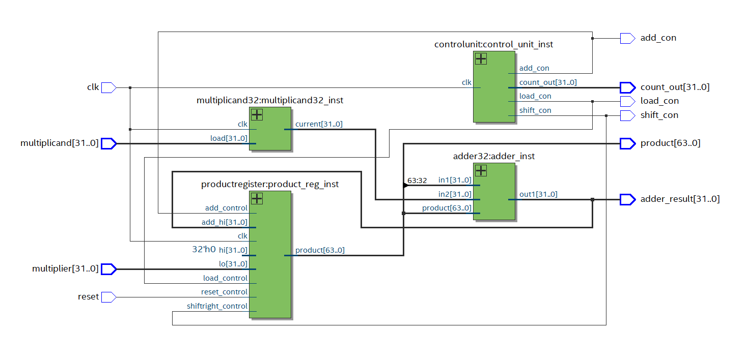 |
The optimized multiply circuit was built with four VHDL units, the product register, the thirty-two-bit adder, the control unit, and the multiplicand register. These components were then connected in the top-level file for the project. Each of the four fundamental VHDL implementations are covered in detail below.
The productregister.vhd implementation is where the control signals enter the data path. The overall implementation has three main control signals: load, add, and shift, all of which enter the data path at the product register. The load control signal is only asserted on startup and populates the product register with the hi and lo values for initialization. The right half of the product register it initialized to the multiplier and the left half is all zeros. Next, the product register is alternated between the add and 3 shift states in that order, for 32 repetitions. In the add state, the high half of the product register is updated with the result of the adder (if LSB is ‘1’), and in turn the adder result is updated, because of the circuit typology and the fact that product(63 downto 32) is an input to the adder. In the shift state, the product register is just shifted to the right one-bit place.
The adder32.vhd implementation simply adds the more significant half of the product register with the multiplicand, in the case that the least significant bit of the product register is one. In the case that the least significant bit of the product register is zero, the most significant half of the product register is passed through to the adder output. This means that in the case that the product register is controlled to add, it will take the result of the adder and place it in the upper half of the product register, and the value will remain unchanged in the case that the least significant bit of the product register is zero, and in the case that the least significant bit is one, it is updated correctly.
The adder32.vhd implementation simply adds the more significant half of the product register with the multiplicand, in the case that the least significant bit of the product register is one. In the case that the least significant bit of the product register is zero, the most significant half of the product register is passed through to the adder output. This means that in the case that the product register is controlled to add, it will take the result of the adder and place it in the upper half of the product register, and the value will remain unchanged in the case that the least significant bit of the product register is zero, and in the case that the least significant bit is one, it is updated correctly.
The controlunit.vhd implementation for this project functions similarly to a simple finite state machine that is initialized in the load state, and on the next clock rising edge jumps to the add state, and then alternates between the add and shift states. The controlunit.vhd implementation has three processes, one functioning as the next state logic, one as the output logic, and the last of the transition logic. The curr_state is initialized to load_state on startup and then is commanded to add_state on the rising edge of the clock. The logic then commands the machine to jump back and forth between add and shift states, for 32 repetitions (one repetition being one add and one shift). The machine is always checking if clock count has reached sixty-five. Sixty-five comes from one clock for the load state, and two clock cycles per repetition inside the finite state machine. As soon as the condition count = sixty-five is reached, the next state is set to end_state, which is a trap state that the system will stay in forever, because there is no exit path from that state. This could actually be improved so that the operations are done in parallel and that would take less clock cycles. If inside the end state, the multiplication has been performed and is complete with the result in the product register. The final process cycles current state to equal next state on every rising clock edge, this keeps the finite state machine moving through states.
The multiplicand register is implemented in the multipicand32.vhd file. This is just a simple register that stores the multiplicand.
The multiplier circuit has a very similar circuit topology to the dedicated multiplier circuit that is part of the MIPS architecture.
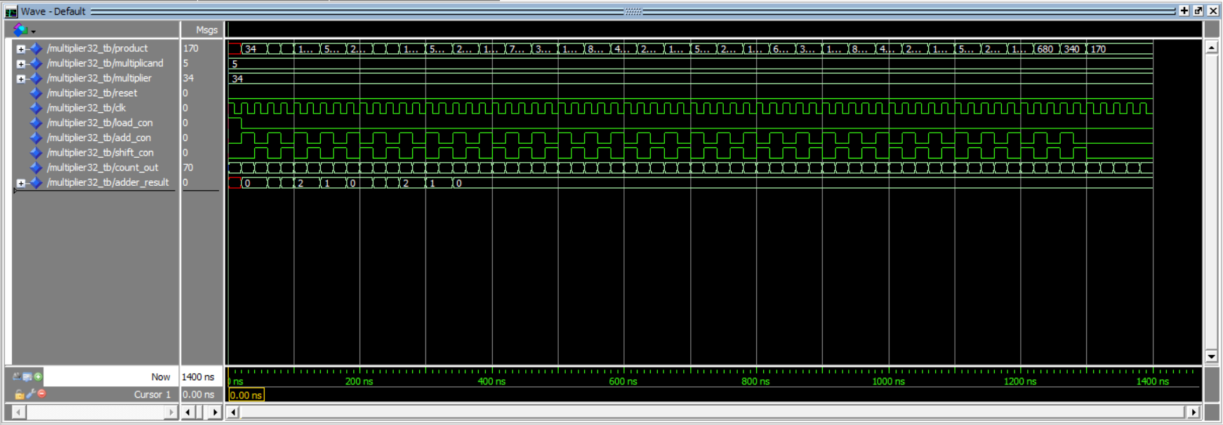
Waveforms:
Below is the ModelSim waveforms that show the circuit values at given clock cycles and the correct value for 5 * 34, 170.
| Image: Waveform |
|---|
 |
Fmax:
The unrestricted Fmax value is 157.28 MHz on the MAX 10 10M50DAF484C6GES FPGA. This just means that the fasted theoretical clock for this system is 157.28 MHz This means that theoretically the multiply operation for any input to this circuit could be computed in 413.3 ns (this comes from (65 clock cycles) * (1/157.28 MHz)) and this would be running at the absolute fastest the circuit can theoretically operate.
ELABORATION ON VHDL FILES INCLUDED:
adder32.vhd - The implementation of the modified 32 bit adder component for the multiply circuit.
adder32_tb.vhd - Testbench written to test the adder operation after the adder was written in VHDL.
controlunit.vhd - Control unit implementation that is used to control the data path of the multiplier circuit.
controlunit_tb.vhd - Testbench written to test the operation of the control unit after it was written in VHDL.
productregister.vhd - VHDL file for the stucture of the product register for the multiplier32 circuit.
productregister_tb.vhd - Testbench written to test the product register immediately after VHDL was written to test the code operation.
multiplicand32.vhd - Multiplicand register file
multiplier32.vhd - The top level file for the project in which all the components are port mapped into the correct configuration to implement the multiplier.
multiplier32_tb.vhd - The testbench for the mulitplier operation that just provided the multiplier and multiplicands and then clock the system to get a result.
NOTE:
The circuit was synthesized in Quartus Prime 20.1. The multiplier.qpf file is included and can be loaded up with the software and the file that can be programmed to a compliant FPGA.